Native Telecom-Band Strong Coupling: A Hardware Architecture for Neutral-Atom Quantum Interconnects

Quantum interconnects distribute entanglement between distant quantum nodes, enabling modular quantum computing and long-distance quantum networks. In this work [1], we demonstrate, to our knowledge, the first neutral-atom cavity-QED system to reach single-atom strong coupling directly on a telecom-band transition. Combining a tunable nanofiber cavity with a reconfigurable 171Yb atom array, we observe collective atom-cavity coupling for up to five atoms and further confirm that the nanofiber region can support more than 100 atoms coupled to the same optical mode. Furthermore, the platform demonstrates key capabilities for QPU integration, including high-fidelity imaging near the nanofiber and atom transport across the device with no measurable loss or heating. Together, these results establish a native hardware architecture that delivers foundational capabilities for both cavity-assisted entanglement generation and seamless QPU integration.
The full paper is available at: https://arxiv.org/abs/2609.25232
The Quantum Interconnect Hardware Challenge
A central challenge for distributed quantum computing and communication is generating remote entanglement at both high rates and high fidelity. Current state-of-the-art experiments with trapped ions achieve entanglement rates on the order of 100 pairs per second [2], whereas proposed fault-tolerant distributed architectures may require 105 pairs/s or more [3]. Closing this gap requires both significantly higher photon collection efficiency and the capability to perform many entanglement attempts in rapid succession and/or in parallel.
An optical cavity addresses the first bottleneck by increasing the probability that an atom emits a photon into a guided optical mode or interacts with an incoming photon. Large, addressable atom arrays can then scale the total entanglement rate through time multiplexing, where multiple atoms sequentially attempt entanglement through a shared optical channel [4, 5].
Nanofiber cavities combine these capabilities within a compact footprint [4]. Their subwavelength diameter tightly confines light near the fiber surface, enabling tweezer-trapped atoms to interact strongly with a telecom-band cavity mode. An extended, uniform waist provides capacity for more than 100 atom sites coupled to a single optical mode for time multiplexing. Additionally, the device’s minimal transverse footprint allows multiple cavities to be positioned within the field of view of the imaging system for spatial multiplexing.
Long-distance quantum links natively benefit from telecom-band photons, which experience minimal loss in optical fiber. Previous single-atom strong-coupling demonstrations with trapped atoms have operated outside the telecom band, thereby requiring quantum frequency conversion for long-distance transmission. A recent free-space experiment with a 171Yb array generated telecom-band atom-photon entanglement and coupled five parallel channels into fiber [6]. However, its reported combined photon collection and transmission efficiency was limited to below 1%, illustrating the fundamental collection challenge that cavity enhancement directly addresses.
First Telecom-Band Strong Coupling
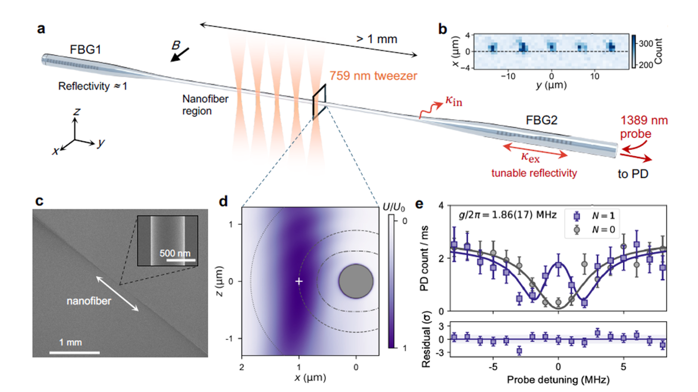
We integrate a 171Yb atom array with a low-loss telecom-band nanofiber cavity, as illustrated in Fig.1a-d. On the native 1389 nm telecom transition, reflection spectroscopy reveals the characteristic splitting of the coupled atom-cavity modes as shown in Fig.1e. Fitting the single-atom spectrum yields an internal cooperativity of Cin = 5.6, establishing single-atom strong coupling in the telecom band. Higher cooperativity generally supports more efficient photon collection and higher-fidelity operations, although full protocol performance also depends on output coupling efficiency, optical loss, and qubit control. We also observe the expected √N scaling for up to five individually trapped atoms, confirming that multiple addressable atoms can share the same optical channel.
We observe comparable peak atom-cavity coupling across a 200 μm region, currently limited by the field of view of the imaging system. The nanofiber itself features a 1 mm uniform-diameter waist, providing capacity for more than 100 atom sites in future implementations.
Accessing High-Fidelity Protocols with Cavity Tunability
The optimal cavity setting depends on the specific networking protocol. In most optical cavities, output coupling is fixed when the mirrors are fabricated. Our device instead uses a thermally tunable fiber Bragg grating as the output mirror, allowing its reflectivity to be dynamically adjusted post-installation.
This mechanism controls light extraction from the cavity over nearly two orders of magnitude while maintaining cavity resonance with the atomic transition. Consequently, a single device can access distinct operational regimes without physical reconfiguration:
- Cavity-assisted photon scattering (CAPS) gates: The demonstrated tuning range includes the impedance-matching condition required for a reflected photon to acquire an atom-state-dependent phase shift while minimizing state-dependent loss [7].
- Cavity-enhanced photon emission: Increasing output mirror transmission directs a larger fraction of cavity-emitted photons into the designated fiber port. Together with high internal cooperativity, these characteristics ensure both efficient photon collection and high state purity in emission-based entanglement protocols.
The tunable output mirror thus enables a single installed nanofiber cavity to satisfy the distinct requirements of both scattering- and emission-based networking schemes.
Compatibility for Neutral-Atom QPU Integration
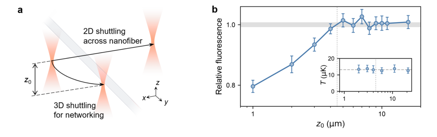
Strong coupling establishes the essential cavity-QED functionality of the interconnect, but integration into a neutral-atom QPU imposes a second, opposing requirement: the physical presence of the nanofiber must remain effectively “invisible” to the atom-array operation. Glass structures near the trapping region can easily disrupt core QPU operations, as scattered excitation light degrades imaging signal-to-noise ratios, while reflected tweezer beams distort trapping potentials and induce heating during transport. We demonstrate that this platform overcomes both risks by validating two key operations adjacent to the nanofiber:
- High-fidelity imaging and stable trapping: Selecting specific propagation directions for the excitation beams suppresses light scattering from the nanofiber surface, keeping background noise low. This geometry yields a site-resolved imaging fidelity of 99.95(6) % for atoms trapped 1 μm from the nanofiber axis. Furthermore, the trap lifetime reaches 6.8(4) s near the nanofiber, showing no measurable degradation compared to atoms held 80 μm away.
- Low-loss atom transport across the nanofiber: Engineering the nanofiber diameter creates destructive interference between surface reflections, minimizing the standing wave pattern in the optical tweezer beam. Consequently, atom arrays are transported in a plane 4.5 μm above the nanofiber axis with no measurable atom loss or heating. Furthermore, this diameter-engineering strategy extends readily to other species; we have confirmed reproducible fabrication at the specific diameters required to suppress reflections for 87Rb, the most widely used species in neutral-atom processors.
These capabilities support a two-layer QPU architecture. Selected atoms approach the cavity for networking operations, while remaining atoms reside in a spatially offset layer for transport, local computation, and storage, enabling the quantum interconnect to interface directly with reconfigurable atom arrays.
Outlook: Scalable Interconnects and Logical Networks
These hardware capabilities lay the groundwork for CAPS gate as a scalable framework for high-rate, high-fidelity quantum networking [7]. By leveraging strong telecom coupling and dynamic cavity impedance matching, the platform natively supports CAPS-based atom-photon entanglement generation at telecom wavelengths. Executing sequential CAPS operations across the addressable atom array enables effective time multiplexing to boost entanglement rates. Furthermore, performing sequential CAPS between remote nodes provides a direct path toward high-fidelity atom-atom entanglement.
Beyond the physical layer, this hardware integrates seamlessly with our theoretical framework for Entanglement Boosting [3], which converts noisy physical Bell pairs into high-fidelity logical Bell pairs. Together, these advances establish a complete roadmap from a physical neutral-atom interface to a logical interconnect for fault-tolerant distributed quantum computing.
References
- H. Ozawa*, N. Chen*, et al., “Strong coupling of a reconfigurable 171Yb atom array to a tunable telecom-band nanofiber cavity” arXiv:2609.25232 (2026)
- L. Stephenson et al., “High-rate, high-fidelity entanglement of qubits across an elementary quantum network,” Phys. Rev. Lett. 124, 110501 (2020).
- S. Sunami*, Y. Hirano*, T. Hinokuma, and H. Yamasaki, “Entanglement boosting: Low-volume logical Bell pair preparation for distributed fault-tolerant quantum computation,” PRX Quantum 7, 033014 (2026).
- S. Horikawa, S. Kato, R. Inoue, T. Aoki, A. Goban, and H. Konishi, “Low-loss telecom-band nanofiber cavity for interfacing Yb atomic qubits,” Opt. Lett. 50, 5294 (2025) .
- S. Sunami, S. Tamiya, R. Inoue, H. Yamasaki and A. Goban, “Scalable networking of neutral-atom qubits: Nanofiber-based approach for multiprocessor fault-tolerant quantum computers,” PRX Quantum 6, 010101 (2025).
- L. Li et al., “Parallelized telecom quantum networking with an ytterbium-171 atom array,” Nature Physics 21, 1826 (2025).
- S. Kikura, K. Tanji, A. Goban and S. Sunami, “Passive quantum interconnects: Multiplexed remote entanglement generation with cavity-assisted photon scattering,” Phys. Rev. Appl. 26, 034021 (2026).